
VLSI Course in Bangalore
Ratings


- Join the Best VLSI Training in Bangalore to Gain In-Depth Knowledge in Chip Design and Semiconductor Technologies.
- Flexible VLSI Training Options: Weekday, Weekend, and Online Batches Available.
- VLSI Training Institute in Bangalore Offering Placement-Focused Coaching with Real-Time Project Exposure.
- Learn Core Topics Like Verilog, VHDL, RTL Design, CMOS Technology, Synthesis, STA, and FPGA Implementation.
- Gain Hands-On Experience Through Practical Labs, Live Design Projects, and Expert-Led Sessions Using Industry Tools.
- Accelerate Career with Resume Building, Mock Interview and Placement Support in VLSI Design and Verification Roles.
Course Duration
50+ HrsLive Project
3 ProjectCertification Pass
GuaranteedTraining Format
Live Online (Expert Trainers)Quality Training With Affordable Fee
 Fees Starts From

11258+
Professionals Trained
10+
Batches every month
3075+
Placed Students
265+
Corporate ServedWhat You'll Learn
Master VLSI Training in Bangalore to learn VLSI design concepts, including digital and analog circuit design techniques.
Gain hands-on experience with industry-standard VLSI tools for simulation and verification.
Understand CMOS technology, fabrication processes, and design flow in VLSI systems.
Master RTL design, FPGA implementation, and timing analysis in VLSI projects.
VLSI Course in Bangalore offers practical sessions for real-world application of concepts.
Boost your career in semiconductor industries with expertise in VLSI design and development.
VLSI Training Objectives
- Digital design
- ASIC and FPGA architectures
- RTL coding, physical design
- Verification techniques
- CAD tools
- Advanced Process Technologies
- System-on-Chip (SoC) Integration
- More Efficient Power Management Techniques
- Increased Use of Artificial Intelligence (AI) in Chip Design
- Development of Quantum Computing Chips
- Cadence Virtuoso
- Synopsys Design Compiler
- Xilinx Vivado
- Mentor Graphics ModelSim
- Emerging technologies
- Design automation
- Hardware security
- System-level design methodologies
Request more informations
WhatsApp (For Call & Chat):
+91 89259 58912
VLSI Course Benefits
VLSI Certification Course in Bangalore offers in-depth training on designing and developing integrated circuits (ICs) using advanced semiconductor technologies. Participants learn about digital and analog circuit design, VLSI architecture, FPGA, ASIC design, and hardware description languages like VHDL and Verilog. The VLSI Course With Placement also covers topics such as testing, fabrication, and verification of VLSI systems. This training equips professionals with the skills needed for careers in electronics, semiconductor industries, and advanced technology development.
- Designation
-
Annual SalaryHiring Companies


Request more informations
WhatsApp (For Call & Chat):
+91 89259 58912
About VLSI Certification Training
Our VLSI Training Institute in Bangalore is designed to provide in-depth knowledge of Very-Large-Scale Integration design, covering digital design, Verilog, RTL design, and physical design flow. Learn from industry professionals through hands-on labs and real-time VLSI Projects in Bangalore. With 500+ hiring partners and 100% VLSI placement support, this course prepares you for a successful career in the semiconductor and chip design industry.
Top Skills You Will Gain
- Digital Design
- RTL Coding
- ASIC Design
- FPGA Programming
- Circuit Simulation
- Timing Analysis
- Synthesis Tools
- Layout Verification
12+ VLSI Tools
Online Classroom Batches Preferred
No Interest Financing start at ₹ 5000 / month
Corporate Training
- Customized Learning
- Enterprise Grade Learning Management System (LMS)
- 24x7 Support
- Enterprise Grade Reporting
Not Just Studying
We’re Doing Much More!
Empowering Learning Through Real Experiences and Innovation


VLSI Training Curriculum
Trainers Profile
Our VLSI Course in Bangalore trainers are certified experts with rich industry backgrounds, currently working in prominent multinational corporations. At Learnovita, they are committed to sharing cutting-edge insights and industry best practices in VLSI, ensuring that learners gain the skills and knowledge needed to succeed. This is further supported through our VLSI Internship in Bangalore, which offers practical experience and prepares students for real-world VLSI roles.
Syllabus of VLSI Course Download syllabus
- Overview of VLSI Technology
- Evolution of Integrated Circuits
- Applications of VLSI
- Challenges in VLSI Design
- PN Junctions and Diodes
- Bipolar Junction Transistors (BJTs)
- CMOS Technology
- Advanced Semiconductor Devices
- Metal-Oxide-Semiconductor Field-Effect Transistors (MOSFETs)
- Combinational Logic Design
- Sequential Logic Design
- Timing Analysis and Clocking
- HDL (Hardware Description Languages)
- Circuit Simulation Tools
- Datapath Design
- Memory Design
- Power Optimization Techniques
- Layout Design and Floorplanning
- System-on-Chip (SoC) Architecture
- Design Abstraction Levels
- Intellectual Property (IP) Cores
- Design for Testability (DFT)
- Silicon Wafer Preparation
- Photolithography
- Etching and Deposition Processes
- Ion Implantation and Doping
- Packaging and Testing
- Amplifier Design Techniques
- Data Converter Design (ADCs, DACs)
- PLL (Phase-Locked Loop) Design
- RF Circuit Design
- ASIC Design Flow
- HDL Coding for ASIC and FPGA
- Place and Route
- FPGA Prototyping and Verification
Request more informations
WhatsApp (For Call & Chat):
+91 89259 58912
REAL

UPGRADE

sowmiya

UPGRADE

Rajkumar

UPGRADE

Thon
UPGRADE

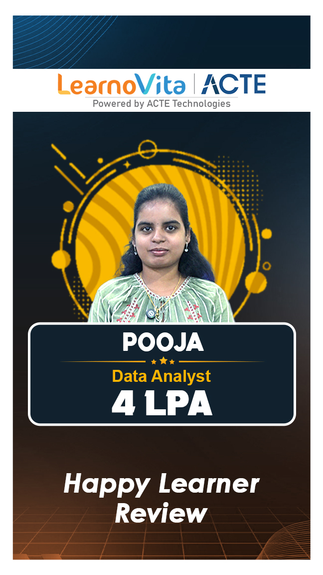
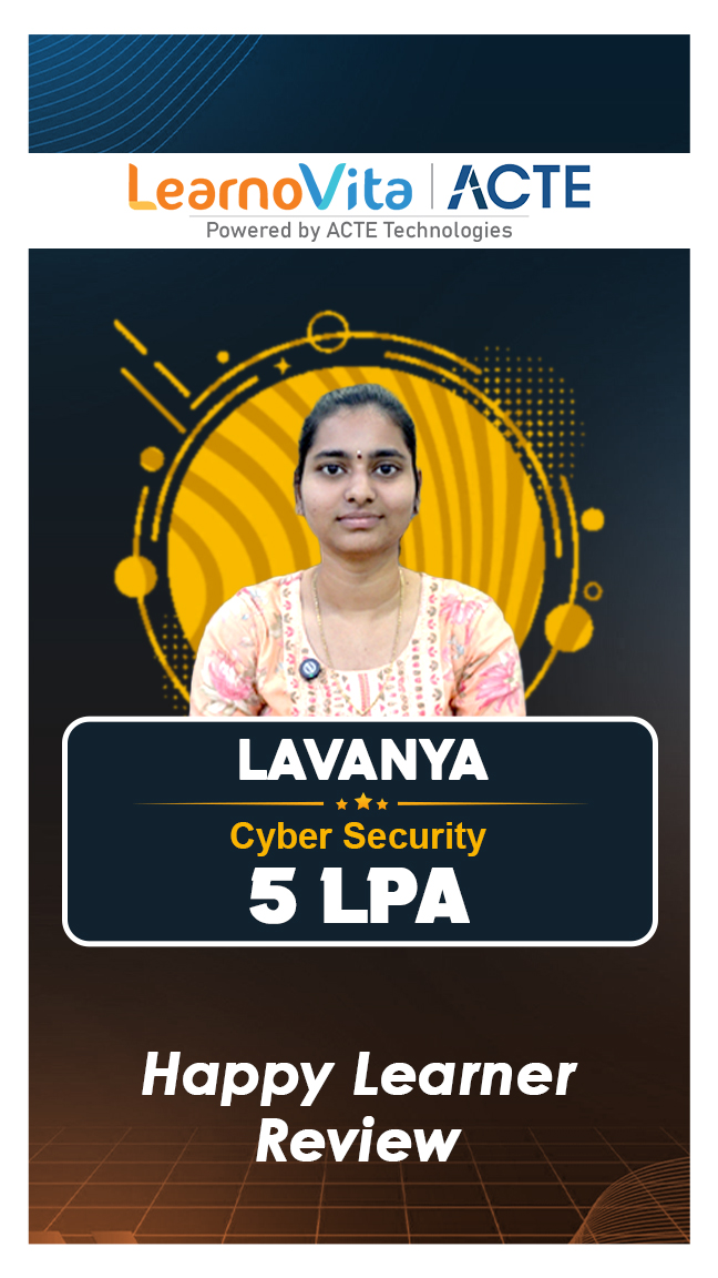
Lavanya

Industry Projects
Exam & VLSI Certification
- Networking events
- Online forums
- Alums associations provide avenues for collaboration
- Knowledge exchange
- Career guidance
- Fostering professional growth
- VLSI certification programs often require participants to trends, tools, and methodologies.
- Continuous learning and recertification ensure that certified professionals remain abreast of evolving VLSI technologies, maintaining their relevance in the dynamic semiconductor landscape.
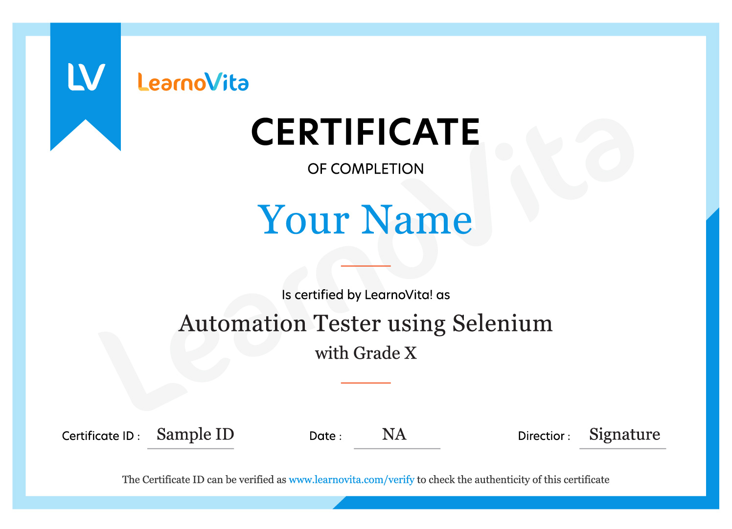
MNC Recognized course
complete certification
Intership
complete certification
Placement
complete certification
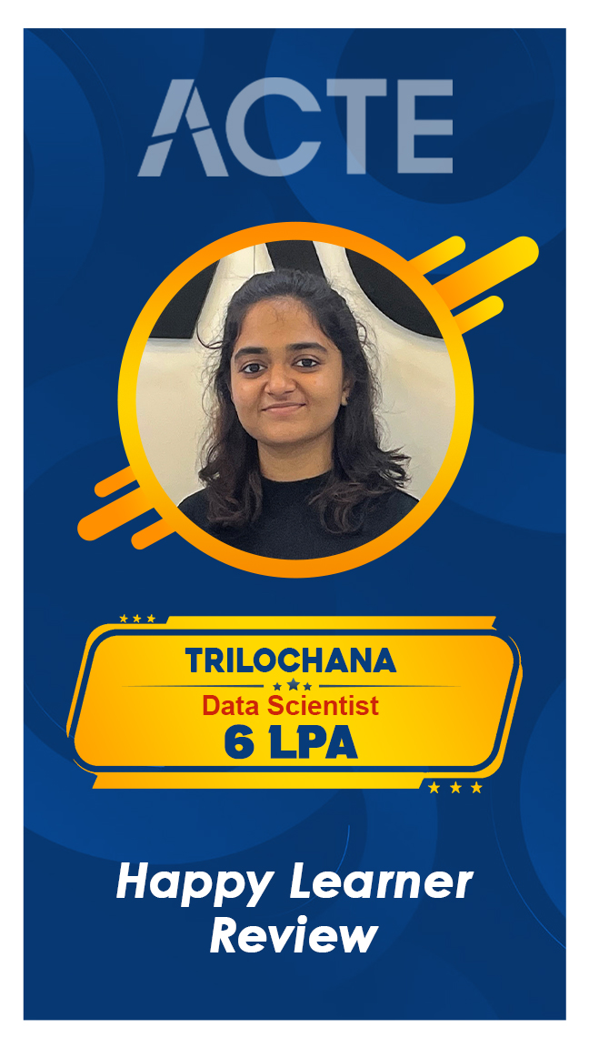
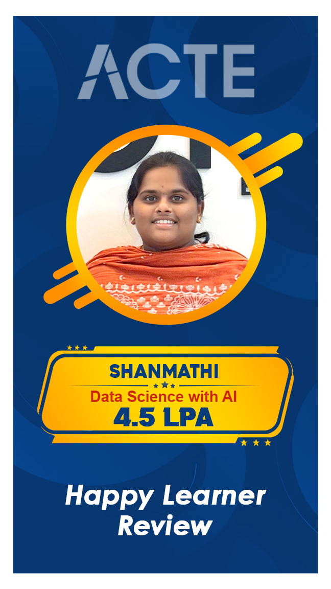
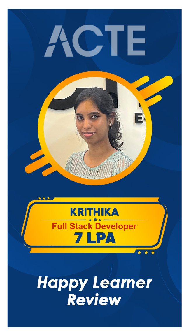
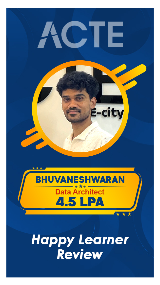
Our learners
transformed their careers

A majority of our alumni
fast-tracked into managerial careers.
Get inspired by their progress in the Career Growth Report.
Our Student Successful Story
 Regular 1:1 Mentorship From Industry Experts
Live Classes
Career Support
Regular 1:1 Mentorship From Industry Experts
Live Classes
Career Support

Sandeep Kumar D
Software Engineer, Cisco Systems )

Vinoth P
UI Developer, TCS
Vijeyalakshme kannan
QA Engineer, Amazon Development Center
Pranav Srinivas
Software Testing, Capgemini
Prasanna
SAP Admin, HCLHow are the VLSI Course with LearnoVita Different?
Feature
LearnoVita
Other Institutes
Affordable Fees
Competitive Pricing With Flexible Payment Options.
Higher VLSI Fees With Limited Payment Options.
Live Class From ( Industry Expert)
Well Experienced Trainer From a Relevant Field With Practical VLSI Training
Theoretical Class With Limited Practical
Updated Syllabus
Updated and Industry-relevant VLSI Course Curriculum With Hands-on Learning.
Outdated Curriculum With Limited Practical Training.
Hands-on projects
Real-world VLSI Projects With Live Case Studies and Collaboration With Companies.
Basic Projects With Limited Real-world Application.
Certification
Industry-recognized VLSI Certifications With Global Validity.
Basic VLSI Certifications With Limited Recognition.
Placement Support
Strong Placement Support With Tie-ups With Top Companies and Mock Interviews.
Basic Placement Support
Industry Partnerships
Strong Ties With Top Tech Companies for Internships and Placements
No Partnerships, Limited Opportunities
Batch Size
Small Batch Sizes for Personalized Attention.
Large Batch Sizes With Limited Individual Focus.
Additional Features
Lifetime Access to VLSI Course Materials, Alumni Network, and Hackathons.
No Additional Features or Perks.
Training Support
Dedicated Mentors, 24/7 Doubt Resolution, and Personalized Guidance.
Limited Mentor Support and No After-hours Assistance.
VLSI Online Course FAQ's
- LearnoVita is dedicated to assisting job seekers in seeking, connecting, and achieving success, while also ensuring employers are delighted with the ideal candidates.
- Upon successful completion of a career course with LearnoVita, you may qualify for job placement assistance. We offer 100% placement assistance and maintain strong relationships with over 650 top MNCs.
- Our Placement Cell aids students in securing interviews with major companies such as Oracle, HP, Wipro, Accenture, Google, IBM, Tech Mahindra, Amazon, CTS, TCS, HCL, Infosys, MindTree, and MPhasis, among others.
- LearnoVita has a legendary reputation for placing students, as evidenced by our Placed Students' List on our website. Last year alone, over 5400 students were placed in India and globally.
- We conduct development sessions, including mock interviews and presentation skills training, to prepare students for challenging interview situations with confidence. With an 85% placement record, our Placement Cell continues to support you until you secure a position with a better MNC.
- Please visit your student's portal for free access to job openings, study materials, videos, recorded sections, and top MNC interview questions.

- Build a Powerful Resume for Career Success
- Get Trainer Tips to Clear Interviews
- Practice with Experts: Mock Interviews for Success
- Crack Interviews & Land Your Dream Job
Global Quality Training
At The Lowest Fees & Expert Trainer


Need custom pricing?