
PCB Design Training in Hyderabad
Ratings


- Join PCB Design Course in Hyderabad to Art of Designing Printed Circuit Boards for Electronics Applications.
- Flexible PCB Design Training Options: Available on Weekday, Weekend, and Fast-Track Batches.
- Top PCB Design Training Institute in Hyderabad Offering Practical Learning with Real-Time Projects.
- Learn Key Topics Including Schematic Capture, PCB Layout, Design Rule Checks, and Gerber File Generation.
- Gain Hands-On Experience Using Industry-Standard Tools like Altium Designer and KiCAD Under Expert Guidance.
- Launch Your Career with Resume Assistance, Interview Preparation, and Dedicated Placement Support.
Course Duration
50+ HrsLive Project
3 ProjectCertification Pass
GuaranteedTraining Format
Live Online (Expert Trainers)Quality Training With Affordable Fee
 Fees Starts From

11568+
Professionals Trained
10+
Batches every month
3126+
Placed Students
289+
Corporate ServedWhat You'll Learn
Use industry-standard EDA tools to learn PCB layout and schematic capture.
Recognize component layout, routing strategies, and signal integrity.
PCB Design Course in Hyderabad Get practical experience creating PCB boards with one or more layers.
For dependable circuit board manufacturing, understand DFM, DFT, and EMC requirements.
Create projects in real time, from conception to the creation of Gerber files.
To get your electronics design career started, enroll in PCB Design Training in Hyderabad.
PCB Design Training Objectives
- Beginning To Advanced PCB Design
- Schematic Design And Capture
- PCB Layout And Routing
- Design Rules And Constraints
- Thermal And Mechanical Design
- PCB Manufacturing Processes
- Testing And Validation
- Understand basic electronics concepts
- Learn essential CAD tools and software
- Develop problem-solving skills
- Familiarize yourself with design rules and constraints
- Prepare for practical design challenges
- Align with industry standards
- Understanding PCB Design Software
- Component Placement Techniques
- Trace Routing Strategies
- Power Supply Design
- Signal Integrity Management
- Multi-Layer PCB Design
Request more informations
WhatsApp (For Call & Chat):
+91 89259 58912
PCB Design Course Benefits
PCB Design Certification Course in Hyderabad provides full understanding on designing printed circuit boards. The PCB Design Internship in Hyderabad topics such schematic capture, layout design, signal integrity, and DFM/DFT guidelines. You will get practical experience with Altium Designer and Eagle, two industry-standard tools.
- Designation
-
Annual SalaryHiring Companies


Request more informations
WhatsApp (For Call & Chat):
+91 89259 58912
About PCB Design Certification Training
Comprehensive knowledge of circuit board design, from schematic capture to layout generation, is provided by our PCB Design Training in Hyderabad. With cutting-edge tools like Altium and Eagle, PCB Design Projects in Hyderabad. The course makes sure you’re ready for issues in the real world by covering topics like signal integrity and DFM requirements. This course provides access to more than 500+ employment partners and PCB Design Course With Placement career in electronics.
Top Skills You Will Gain
- Schematic Capture
- Layout Design
- Signal Integrity
- Component Placement
- Routing Techniques
- DFM Guidelines
- PCB Simulation
- Gerber File
12+ PCB Design Tools
Online Classroom Batches Preferred
No Interest Financing start at ₹ 5000 / month
Corporate Training
- Customized Learning
- Enterprise Grade Learning Management System (LMS)
- 24x7 Support
- Enterprise Grade Reporting
Not Just Studying
We’re Doing Much More!
Empowering Learning Through Real Experiences and Innovation


PCB Design Course Curriculum
Trainers Profile
Our PCB Design Course trainers are seasoned professionals with expertise in electronics in industries such as consumer electronics, telecommunications, automotive, and aerospace. They offer practical insights, use industry-standard software, and provide up-to-date training on PCB design, fabrication, and testing. Our PCB Design Course trainers bring real-world experience from top industries and guide students with hands-on skills, including PCB design internship opportunities.
Syllabus of PCB Design Course Download syllabus
- Overview of PCB Design
- PCB Design Flow
- Types of PCBs Like Single, Double, and Multi-Layer
- Basic PCB Components
- PCB Design Tools and Software
- Applications of PCBs
- Introduction to PCB Design Software
- Installation and Setup
- Creating and Managing Schematics
- PCB Layout Design Features
- Simulation and Analysis Tool
- Understanding PCB Fundamentals
- Types of PCBs and Their Applications
- Basic PCB Design Terminology
- Introduction to PCB Layers and Stackups
- Component Placement and Orientation
- Basic Routing Techniques
- Creating Schematics
- Component Selection
- Wiring and Connections
- Schematic Symbols and Libraries
- Annotating and Labeling Components
- Design Rule Checks (DRC) in Schematics
- Component Placement
- Trace Routing
- Via and Hole Placement
- Layer Management
- Design Rule Check (DRC)
- Signal Integrity Considerations
- Power and Ground Plane Design
- Overview of PCB Manufacturing
- Types of PCB Materials
- Fabrication Techniques
- Understanding Gerber Files
- Photolithography Process
- Etching and Plating
- Drilling and Routing
- Types of PCB Assembly
- Soldering Techniques
- Surface Mount vs. Through-Hole Technology
- Component Placement
- Reflow Soldering Process
- Wave Soldering Process
- Importance of Signal Integrity
- Signal Integrity Concepts and Terminology
- Minimizing Signal Interference
- Controlling Impedance
- Signal Trace Routing Techniques
- Grounding and Decoupling Strategies
- Use of Differential Pairs
- Designing Power and Ground Planes
- Decoupling Capacitors Placement
- Minimizing Power Noise
- Ensuring Adequate Power Distribution
- Designing for Thermal Management
- Optimizing Plane Layer Stackup
- Heat Dissipation Techniques
- Thermal Analysis Tools and Methods
- Designing for Effective Heat Management
- Thermal Via and Pad Design
- Use of Heat Sinks and Thermal Pads
- Thermal Simulation and Modeling
Request more informations
WhatsApp (For Call & Chat):
+91 89259 58912
REAL

UPGRADE

sowmiya

UPGRADE

Rajkumar

UPGRADE

Thon
UPGRADE

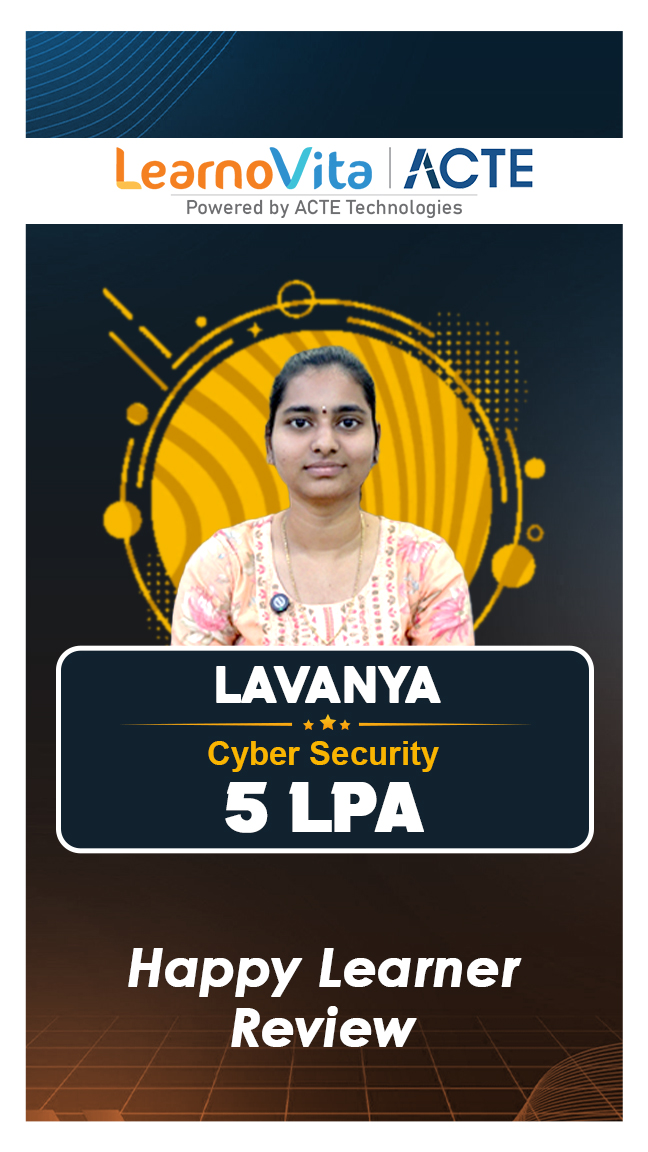
Lavanya

Industry Projects
Exam & PCB Design Certification
- Enroll in our PCB Design training program
- Practice with design exercises and project design
- Gain hands-on experience with PCB design tools
- Utilize supplementary study materials and guides
- Enhanced Career Opportunities
- Industry Recognition
- Increases Earning Potential
- Professional Credibility
- Skill Validation
- Networking Opportunities
MNC Recognized course
complete certification
Intership
complete certification
Placement
complete certification
Our learners
transformed their careers

A majority of our alumni
fast-tracked into managerial careers.
Get inspired by their progress in the Career Growth Report.
Our Student Successful Story
 Regular 1:1 Mentorship From Industry Experts
Live Classes
Career Support
Regular 1:1 Mentorship From Industry Experts
Live Classes
Career Support

Sandeep Kumar D
Software Engineer, Cisco Systems )

Vinoth P
UI Developer, TCS
Vijeyalakshme kannan
QA Engineer, Amazon Development Center
Pranav Srinivas
Software Testing, Capgemini
Prasanna
SAP Admin, HCLHow are the PCB Design Course with LearnoVita Different?
Feature
LearnoVita
Other Institutes
Affordable Fees
Competitive Pricing With Flexible Payment Options.
Higher PCB Design Fees With Limited Payment Options.
Live Class From ( Industry Expert)
Well Experienced Trainer From a Relevant Field With Practical PCB Design Training
Theoretical Class With Limited Practical
Updated Syllabus
Updated and Industry-relevant PCB Design Course Curriculum With Hands-on Learning.
Outdated Curriculum With Limited Practical Training.
Hands-on projects
Real-world PCB Design Projects With Live Case Studies and Collaboration With Companies.
Basic Projects With Limited Real-world Application.
Certification
Industry-recognized PCB Design Certifications With Global Validity.
Basic PCB Design Certifications With Limited Recognition.
Placement Support
Strong Placement Support With Tie-ups With Top Companies and Mock Interviews.
Basic Placement Support
Industry Partnerships
Strong Ties With Top Tech Companies for Internships and Placements
No Partnerships, Limited Opportunities
Batch Size
Small Batch Sizes for Personalized Attention.
Large Batch Sizes With Limited Individual Focus.
Additional Features
Lifetime Access to PCB Design Course Materials, Alumni Network, and Hackathons.
No Additional Features or Perks.
Training Support
Dedicated Mentors, 24/7 Doubt Resolution, and Personalized Guidance.
Limited Mentor Support and No After-hours Assistance.
PCB Design Course FAQ's
- LearnoVita is dedicated to assisting job seekers in seeking, connecting, and achieving success, while also ensuring employers are delighted with the ideal candidates.
- Upon successful completion of a career course with LearnoVita, you may qualify for job placement assistance. We offer 100% placement assistance and maintain strong relationships with over 650 top MNCs.
- Our Placement Cell aids students in securing interviews with major companies such as Oracle, HP, Wipro, Accenture, Google, IBM, Tech Mahindra, Amazon, CTS, TCS, HCL, Infosys, MindTree, and MPhasis, among others.
- LearnoVita has a legendary reputation for placing students, as evidenced by our Placed Students' List on our website. Last year alone, over 5400 students were placed in India and globally.
- We conduct development sessions, including mock interviews and presentation skills training, to prepare students for challenging interview situations with confidence. With an 85% placement record, our Placement Cell continues to support you until you secure a position with a better MNC.
- Please visit your student's portal for free access to job openings, study materials, videos, recorded sections, and top MNC interview questions.

- Build a Powerful Resume for Career Success
- Get Trainer Tips to Clear Interviews
- Practice with Experts: Mock Interviews for Success
- Crack Interviews & Land Your Dream Job
Global Quality Training
At The Lowest Fees & Expert Trainer


Need custom pricing?